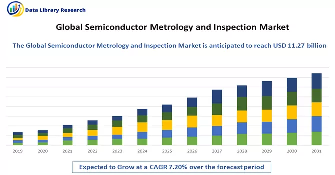
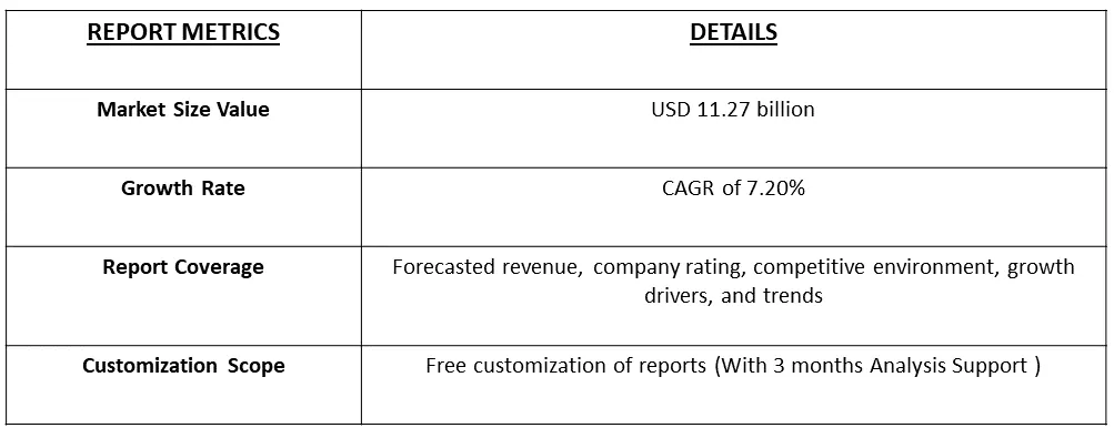
The Semiconductor Metrology And Inspection Equipment Market size is estimated at USD 11.27 billion in 2024 and is a CAGR of 7.20% during the forecast period 2024-2031.
Get Complete Analysis Of The Report - Download Free Sample PDF
Semiconductor metrology and inspection refer to the set of processes and techniques employed in the semiconductor manufacturing industry to measure, analyze, and ensure the quality of semiconductor devices and components. These processes are crucial for maintaining the precision and integrity of semiconductor manufacturing, where tiny structures and features are produced on semiconductor wafers to create integrated circuits and other electronic components. Metrology involves the measurement of critical dimensions, thicknesses, and other parameters to ensure that the fabricated structures meet the required specifications. Inspection, on the other hand, involves the examination of the semiconductor materials and devices to detect defects, contamination, or irregularities that could affect their functionality. Advanced tools such as scanning electron microscopes (SEM), atomic force microscopes (AFM), and optical inspection systems are commonly used for semiconductor metrology and inspection. These processes play a vital role in achieving high yields, improving production efficiency, and ensuring the overall reliability and performance of semiconductor devices in various electronic applications.
The semiconductor metrology and inspection market is witnessing notable growth, propelled by continuous advancements in semiconductor manufacturing. The industry's shift towards smaller nodes and 3D packaging has intensified the demand for sophisticated metrology and inspection tools crucial for ensuring precision in the production of intricate semiconductor devices. The increasing complexity of these devices, alongside consumer preferences for compact and high-performance electronics, emphasizes the pivotal role of advanced measurement and inspection techniques. Stringent quality control standards, the global expansion of the semiconductor market, and the incorporation of artificial intelligence (AI) and machine learning (ML) into these tools for real-time insights and predictive maintenance contribute to market growth.
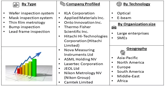
Market Segmentation: The Global Semiconductor Metrology & Inspection System Market is segmented by type (lithography metrology (overlay, dimension equipment, and mask inspection/metrology), wafer inspection, thin film metrology, other types), and geography (North America, Europe, Asia Pacific, and Rest of The World). The market size and forecasts are provided in terms of value (USD million) for all the above segments.
For Detailed Market Segmentation - Download Free Sample PDF
The growing complexity of semiconductor designs, notably with the emergence of 3D structures and advanced packaging technologies, is generating an increased need for advanced metrology and inspection systems. This demand arises from the essential requirement to validate the intricate patterns and structures inherent in these sophisticated semiconductor designs. In the dynamic landscape of evolving technology, the semiconductor industry heavily depends on cutting-edge metrology tools to guarantee precision and accuracy in verifying the nuanced details associated with 3D structures and advanced packaging methodologies. These highly sophisticated systems serve as integral components of quality control processes, playing a pivotal role in ensuring the production of high-performance semiconductor devices. Their capability to meticulously inspect and measure intricate features contributes significantly to maintaining the stringent standards required for modern semiconductor manufacturing.
Market Drivers:
Increasing Demand for High-performance, Low-cost Semiconductors
The increasing demand for high-performance, low-cost semiconductors is a prominent trend driven by various factors shaping the technology landscape. In today's digital era, where electronic devices are ubiquitous, there is a growing need for semiconductors that offer enhanced performance without compromising affordability. This surge in demand is propelled by several key factors. Firstly, the rapid expansion of emerging technologies such as 5G, the Internet of Things (IoT), artificial intelligence (AI), and autonomous vehicles necessitates semiconductor solutions that can meet the heightened performance requirements of these applications. Additionally, the proliferation of consumer electronics, ranging from smartphones to smart home devices, contributes to the escalating demand for cost-effective yet powerful semiconductors to power these devices. The global push for digital transformation across industries further amplifies the call for semiconductors that strike a balance between performance and cost-effectiveness. This demand is particularly pronounced in sectors like healthcare, automotive, and industrial applications, where high-performance semiconductors are essential for driving innovation and efficiency. Thus, such factors are expected to drive the growth of the studied market over the forecast period.
Increasing Demand for Semiconductor Wafers in Consumer Electronics
The increasing demand for semiconductor wafers in consumer electronics is a significant trend propelled by the relentless evolution of technology and the ubiquitous integration of electronic devices into daily life. Consumer electronics, including smartphones, tablets, smartwatches, and smart home devices, rely heavily on semiconductor components to deliver enhanced performance and advanced functionalities. As consumer expectations for faster processors, increased memory capacity, and energy-efficient devices rise, the demand for semiconductor wafers, the foundational substrate for semiconductor manufacturing, continues to soar. This surge is driven by the need for cutting-edge microprocessors, memory chips, and integrated circuits that power the latest features in electronic gadgets. The growing popularity of high-performance computing, artificial intelligence, and 5G connectivity further fuels the demand for advanced semiconductor wafers, as these technologies require sophisticated and efficient semiconductor components. As a result, semiconductor manufacturers are investing in innovative fabrication technologies, such as advanced lithography and 3D stacking, to meet the demand for smaller, more powerful, and energy-efficient devices in the consumer electronics market. The increasing integration of semiconductor wafers in consumer electronics underscores their pivotal role in shaping the landscape of modern technology and meeting the escalating expectations of tech-savvy consumers worldwide.
Market Restraints:
High Setup Cost and Lack of Expertise in Handling Metrology Systems Efficiently
The semiconductor metrology market faces potential challenges due to high setup costs and a potential lack of expertise in handling metrology systems efficiently. The sophisticated nature of metrology tools, which are essential for precise measurements and inspections in semiconductor manufacturing, often requires substantial investments in infrastructure and equipment setup. The initial costs associated with acquiring and implementing these advanced metrology systems can be significant, posing a barrier to entry for some companies, particularly smaller enterprises. Additionally, the complexity of these systems necessitates a skilled workforce with expertise in operating and maintaining them effectively. The shortage of qualified professionals capable of handling intricate metrology tools may hinder the seamless integration and utilization of these systems in semiconductor manufacturing processes.
The COVID-19 pandemic has had a notable impact on the semiconductor metrology market. Disruptions in global supply chains, lockdowns, and restrictions on manufacturing facilities have led to delays and uncertainties in semiconductor production. The semiconductor industry faced challenges such as fluctuations in demand, workforce disruptions, and supply chain interruptions. Consequently, these factors have influenced the adoption and implementation of metrology solutions. While the pandemic underscored the importance of resilient supply chains and agile manufacturing processes, it also accelerated digital transformation initiatives in the semiconductor sector. The increased focus on remote monitoring, data analytics, and automation has driven the demand for advanced metrology tools to enhance precision and efficiency in semiconductor manufacturing. As the industry navigates through recovery, the semiconductor metrology market is poised to play a crucial role in supporting innovation and ensuring the quality and reliability of semiconductor devices.
Segmental Analysis:
Lithography Metrology Segment is Expected to Witness Significant Growth Over the Forecast Period
Lithography metrology plays a pivotal role in semiconductor manufacturing, particularly in the fabrication of integrated circuits and other semiconductor devices. Lithography is a key step in the semiconductor manufacturing process where patterns are transferred onto silicon wafers using techniques like photolithography. Lithography metrology involves precise measurements and inspections during this critical step to ensure the accuracy, uniformity, and quality of the patterns. Advanced metrology tools are employed to measure critical dimensions, overlay accuracy, and other parameters, ensuring that the lithographic process meets the stringent requirements of modern semiconductor designs. These metrology techniques are crucial in maintaining the integrity of shrinking feature sizes and increasing device complexity. As the semiconductor industry continues to advance with smaller nodes and more intricate designs, lithography metrology remains indispensable for achieving high yields and manufacturing reliable, high-performance semiconductor devices. Continuous innovation in lithography metrology tools is essential to meet the evolving demands of the semiconductor market and support the development of cutting-edge technologies.
Asia-Pacific Region is Expected to Witness Significant Growth Over the Forecast Period
The Asia Pacific region stands as a pivotal force in the global semiconductor metrology market, driven by its robust semiconductor manufacturing landscape and continual technological advancements. Countries like China, Japan, South Korea, Taiwan, and Singapore contribute significantly to the region's prominence in semiconductor production. With a strong emphasis on manufacturing prowess, technological innovation, and substantial investments in research and development, Asia Pacific holds a central position in the adoption of advanced metrology tools. The region's booming consumer electronics market, coupled with the rising demand for advanced technologies like 5G and artificial intelligence, further fuels the need for precise semiconductor manufacturing, emphasizing the critical role of metrology solutions. Strategic alliances and collaborations within the industry contribute to knowledge exchange and technology transfer, reinforcing the region's influence in shaping the global semiconductor landscape. As Asia Pacific continues to be a driving force in semiconductor manufacturing, its impact on the semiconductor metrology market remains pivotal for ensuring precision, quality, and technological excellence.
Get Complete Analysis Of The Report - Download Free Sample PDF
In the arena of semiconductor metrology and inspection equipment, key players like Applied Materials Inc., Nikon Metrology NV, and KLA Corporation hold prominent positions. These companies have consistently augmented their operational footprints through strategic market expansions and acquisitions, playing a pivotal role in steering the overall market growth. The initiation of acquisition activities has proven instrumental in propelling advancements and expansion within the market. Notably, these industry leaders have allocated substantial resources to research and development endeavors, safeguarding their market standing and fostering innovation within the sector. The competitive landscape remains intense, primarily attributed to the robust presence of these major players shaping the trajectory of the semiconductor metrology and inspection equipment market. A few key market players are:
Recent Developments:
1) In December 2023, Hitachi High-Tech Corporation introduced the GT2000 high-precision electron beam metrology system, leveraging its extensive expertise in Critical Dimension Scanning Electron Microscopy (CD-SEM), where it holds a leading market position. The GT2000 is specifically designed with advanced detection systems tailored for 3D semiconductor devices, showcasing its dedication to cutting-edge technology. Notably, it features low-damage, high-speed multi-point measurement capabilities for imaging high-NA EUV resist wafers, aiming to minimize resist damage and enhance yield in mass production. The introduction of the Hitachi High-Tech GT2000 CD-SEM aims to revolutionize the manufacturing process of intricate semiconductor devices, enabling high-precision, high-speed measurements and inspections. This development addresses the challenges posed by the ongoing miniaturization and complexity of advanced semiconductor devices, making a significant contribution to improved customer yields in both research and development and large-scale production environments.
2) In July 2023, Applied Materials Inc. unveiled a suite of materials, technologies, and systems geared towards assisting chipmakers in seamlessly integrating chiplets into advanced 2.5D and 3D packages through the utilization of hybrid bonding and through-silicon vias (TSVs). This groundbreaking introduction signifies Applied Materials' commitment to advancing its already extensive portfolio of technologies tailored for heterogeneous integration (HI). As the foremost supplier of HI technologies, the company offers a comprehensive range of optimized chipmaking systems, encompassing etch, physical and chemical vapor deposition (PVD), electroplating, chemical mechanical polishing (CMP), annealing, and surface treatments. This strategic move positions Applied Materials at the forefront of innovation, empowering chipmakers with cutting-edge solutions to navigate the complexities of modern semiconductor integration.
Q1. What is the current Semiconductor Metrology and Inspection Market size?
As per Data Library Research the Semiconductor Metrology And Inspection Equipment Market size is estimated at USD 11.27 billion.
Q2. At what CAGR is the Semiconductor Metrology And Inspection Equipment Market projected to grow within the forecast period?
Semiconductor Metrology And Inspection Equipment Market is a CAGR of 7.20% during the forecast period.
Q3. What are the Growth Drivers of the Semiconductor Metrology And Inspection Equipment Market?
Increasing Demand for High-performance, Low-cost Semiconductors and Increasing Demand for Semiconductor Wafers in Consumer Electronics are the Growth Drivers of the Semiconductor Metrology And Inspection Equipment Market.
Q4. Which region has the largest share of the Semiconductor Metrology And Inspection Equipment market? What are the largest region's market size and growth rate?
Asia Pacific Market has the largest share of the market. For detailed insights on the largest region's market size and growth rate request a sample here.
Data Library Research are conducted by industry experts who offer insight on industry structure, market segmentations technology assessment and competitive landscape (CL), and penetration, as well as on emerging trends. Their analysis is based on primary interviews (~ 80%) and secondary research (~ 20%) as well as years of professional expertise in their respective industries. Adding to this, by analysing historical trends and current market positions, our analysts predict where the market will be headed for the next five years. Furthermore, the varying trends of segment & categories geographically presented are also studied and the estimated based on the primary & secondary research.
In this particular report from the supply side Data Library Research has conducted primary surveys (interviews) with the key level executives (VP, CEO’s, Marketing Director, Business Development Manager and SOFT) of the companies that active & prominent as well as the midsized organization
FIGURE 1: DLR RESEARH PROCESS
Extensive primary research was conducted to gain a deeper insight of the market and industry performance. The analysis is based on both primary and secondary research as well as years of professional expertise in the respective industries.
In addition to analysing current and historical trends, our analysts predict where the market is headed over the next five years.
It varies by segment for these categories geographically presented in the list of market tables. Speaking about this particular report we have conducted primary surveys (interviews) with the key level executives (VP, CEO’s, Marketing Director, Business Development Manager and many more) of the major players active in the market.
Secondary ResearchSecondary research was mainly used to collect and identify information useful for the extensive, technical, market-oriented, and Friend’s study of the Global Extra Neutral Alcohol. It was also used to obtain key information about major players, market classification and segmentation according to the industry trends, geographical markets, and developments related to the market and technology perspectives. For this study, analysts have gathered information from various credible sources, such as annual reports, sec filings, journals, white papers, SOFT presentations, and company web sites.
Market Size EstimationBoth, top-down and bottom-up approaches were used to estimate and validate the size of the Global market and to estimate the size of various other dependent submarkets in the overall Extra Neutral Alcohol. The key players in the market were identified through secondary research and their market contributions in the respective geographies were determined through primary and secondary research.
Forecast Model