3D Wafer Bump Inspection System Market Overview and Analysis:
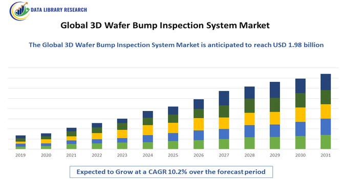
- The Global 3D Wafer Bump Inspection System Market, essential for advanced semiconductor packaging, was valued at approximately USD 702.2 million in 2024. It is projected to grow to about USD 1.98 billion by 2032, expanding at a Compound Annual Growth Rate (CAGR) of roughly 10.2% during this period.
Get Complete Analysis Of The Report - Download Updated Free Sample PDF
The Global 3D Wafer Bump Inspection System Market is experiencing strong growth, driven primarily by the rising demand for advanced semiconductor devices, increasing adoption of miniaturized electronic components, and the rapid expansion of consumer electronics, automotive electronics, and IoT applications. As wafer-level packaging and fine-pitch bump structures become more complex, manufacturers require highly precise, high-resolution 3D inspection systems to ensure defect-free production and maintain yield efficiency.
3D Wafer Bump Inspection System Market Latest Trends
The Global 3D Wafer Bump Inspection System Market is witnessing a shift toward high-precision, automated inspection solutions that leverage advanced imaging technologies such as optical, X-ray, and laser-based metrology. Manufacturers are increasingly adopting AI and machine learning algorithms to enhance defect detection accuracy, reduce false positives, and enable predictive maintenance in semiconductor fabrication. There is also a growing trend of inline and real-time inspection systems, which allow for faster throughput and minimal production downtime, addressing the needs of high-volume wafer-level packaging and fine-pitch bump processes.
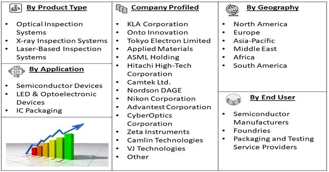
Segmentation: Global 3D Wafer Bump Inspection System Market is segmented By Type (Optical Inspection Systems, X-ray Inspection Systems, Laser-Based Inspection Systems), Application (Semiconductor Devices, LED & Optoelectronic Devices, IC Packaging), End User (Semiconductor Manufacturers, Foundries, Packaging and Testing Service Providers), and Geography (North America, Europe, Asia-Pacific, Middle East and Africa, and South America). The report provides the value (in USD million) for the above segments.
For Detailed Market Segmentation - Get a Free Sample PDF
Market Drivers:
- Rising Demand for Advanced Semiconductor Devices
The growing adoption of high-performance semiconductor devices in consumer electronics, automotive electronics, 5G infrastructure, AI chips, and IoT applications is a major driver for the 3D wafer bump inspection system market. As semiconductor devices become more compact, with finer bump pitches and higher density packaging, ensuring defect-free production is critical. For instance, Government of India, reported that, India’s semiconductor market is projected to reach USD 100–110 billion by 2030, driven by the INR 76,000 crore India Semiconductor Mission. With four new units approved on August 12, 2025, totaling Rs.4,600 crore, cumulative investments now reach Rs.1.60 lakh crore across six states. Events like SEMICON India 2025 and global participation underscore rising demand for advanced semiconductor devices, boosting the global 3D wafer bump inspection system market.
3D wafer bump inspection systems provide precise, high-resolution inspection capabilities to detect voids, misalignments, and other defects at an early stage. This ensures higher yield, reduces wastage, and maintains product reliability, which is essential for industries that demand high-quality, high-performance chips.
- Increasing Adoption of Wafer-Level Packaging and Automation
The trend toward wafer-level packaging (WLP), flip-chip technology, and heterogeneous integration is driving demand for advanced inspection solutions. WLP and 3D ICs involve complex multi-layer structures with fine-pitch bumps, making conventional inspection methods insufficient. 3D wafer bump inspection systems allow automated, inline, and real-time defect detection, improving production efficiency and reducing downtime. The push toward automated semiconductor manufacturing further accelerates the adoption of these systems, as manufacturers seek reliable, high-throughput inspection solutions that integrate seamlessly into modern fabrication lines.
Market Restraints
- High Cost of Advanced Inspection Systems
3D wafer bump inspection systems, especially those using X-ray or laser-based technologies, involve significant capital investment. The equipment requires high-precision optics, sensors, sophisticated imaging software, and automation integration, making it expensive to procure and maintain. Small and medium-sized semiconductor manufacturers or foundries may find it challenging to justify these costs, particularly if their production volumes are lower. High upfront costs can slow market adoption, especially in regions where cost sensitivity is a critical factor.
Socioeconomic Impact on 3D Wafer Bump Inspection System Market
The global 3D wafer bump inspection system market has significant socioeconomic impacts. By improving the quality and reliability of semiconductors, these systems support the production of advanced electronics, including smartphones, computers, and automotive components, which are vital for modern life. Higher-quality chips reduce product failures, saving costs for manufacturers and consumers. The market also creates skilled jobs in engineering, manufacturing, and research, driving economic growth. Furthermore, innovations in wafer inspection contribute to technological progress, enabling smarter devices and more efficient industrial processes. Overall, the market strengthens economies, enhances technology access, and supports employment in high-tech sectors worldwide.
Segmental Analysis:
- X-ray Inspection Systems segment is expected to witness the highest growth over the forecast period
X-ray inspection systems are the most widely adopted technology for 3D wafer bump inspection due to their ability to detect internal defects, voids, misalignments, and solder joint issues that are not visible with optical inspection. These systems are essential for high-density, fine-pitch wafer-level packaging and flip-chip applications, ensuring high yield and reliability in advanced semiconductor devices.
- Semiconductor Devices segment is expected to witness the highest growth over the forecast period
The semiconductor devices segment dominates the application category, as wafers used in microprocessors, memory chips, and logic devices require precise bump inspection to maintain performance and reliability. Increasing demand for high-performance computing, AI chips, and 5G-enabled devices is driving the need for rigorous quality control using 3D inspection systems.
- Semiconductor Manufacturers segment is expected to witness the highest growth over the forecast period
Semiconductor manufacturers are the primary end users of 3D wafer bump inspection systems, leveraging these solutions to ensure defect-free production, maintain high yields, and reduce scrap rates. These systems are critical in fabs and fabrication facilities where quality control directly impacts production efficiency and profitability.
- Asia-Pacific region is expected to witness the highest growth over the forecast period
The Asia-Pacific region is expected to witness the highest growth in the global 3D wafer bump inspection system market over the forecast period. Rapid expansion of semiconductor manufacturing, particularly in countries like China, South Korea, and Taiwan, is driving demand for advanced inspection systems. For instance, in 2021, Onto Innovation’s launch of the Dragonfly G3 inspection platform, delivered to leading OSAT and CMOS image sensor manufacturers, enhanced advanced 2D and 3D inspection capabilities. This development strengthened the Asia-Pacific 3D wafer bump inspection system market by improving precision, supporting high-tech semiconductor production, and driving regional adoption of advanced packaging technologies.
Rising adoption of advanced packaging technologies, increasing production of memory, logic, and image sensor chips, and government support for high-tech manufacturing further fuel market growth. Additionally, the presence of leading OSATs and semiconductor companies in the region accelerates innovation and deployment of 3D inspection solutions. These factors collectively position Asia-Pacific as the fastest-growing market globally.
| Report Matrics |
Details |
| Market Size Value |
USD 1.98 billion |
| Growth Rate |
CAGR of 10.2 % |
| Forecast |
2026-2033 |
| Historical data |
2021-2024 |
| Base Year |
2025 |
| Report Coverage |
Forecasted revenue, company rating, competitive environment, growth drivers, and trends |
| Segment Coverage |
Type, Application, End-User, Geography |
| Regional Scope |
North America, Europe, Asia Pacific, Middle East |
| Customized scope |
Free customization of reports (With 3 months Analysis Support ) |
| To Learn More About This Report |
Request a Free Sample Copy |
3D Wafer Bump Inspection System Market Competitive Landscape
The Global 3D Wafer Bump Inspection System Market is highly competitive, characterized by continuous innovation, technological advancements, and strategic partnerships among key players. Companies are focusing on enhancing inspection accuracy, throughput, and automation capabilities to meet the growing demands of semiconductor manufacturers, foundries, and packaging service providers. The market is driven by the development of high-resolution X-ray, optical, and laser-based inspection systems that can handle complex, fine-pitch wafer-level packaging and multi-layer semiconductor devices. Additionally, investment in R&D for AI-assisted defect detection, inline inspection, and real-time process monitoring is helping companies differentiate their offerings and expand their presence in major semiconductor manufacturing regions.
Key Players:
- KLA Corporation
- Onto Innovation
- Tokyo Electron Limited
- Applied Materials
- ASML Holding
- Hitachi High-Tech Corporation
- Camtek Ltd.
- Nordson DAGE
- Nikon Corporation
- Advantest Corporation
- CyberOptics Corporation
- Zeta Instruments
- Camlin Technologies
- Besi (BE Semiconductor Industries)
- FEI Company (Thermo Fisher Scientific)
- VJ Technologies
- Toray Engineering
- Omron Corporation
- Nova Measuring Instruments
- Rudolph Technologies
Recent Development
- In October 2025, Nordson Test & Inspection showcased its advanced semiconductor inspection solutions at Productronica and SEMICON Europa in Munich. Demonstrations included WaferSense sensors, SQ5000 Pro multi-function system, Quadra Pro MXI, Gen 7 AMI, and X3 AXI with Dynamic Planar CT, highlighting the company’s innovations in wafer and electronic component inspection technologies.
- In September 2025, ViTrox, aiming to be the world’s most trusted technology company, participated with Sales Channel Partners Maxim SMT and Bergen Group at India’s leading exhibitions. The company showcased its solutions at SEMICON India 2025 in New Delhi and Productronica India 2025 in Bengaluru, highlighting innovations in semiconductor and electronics inspection technologies.
Frequently Asked Questions (FAQ) :
Q1. What are the main growth-driving factors for this market?
The main driver is the growing demand for smaller, more complex, and high-performance semiconductor devices, especially in areas like 5G, AI, and automotive electronics. These advanced chips require 3D packaging and tiny "bumps" (interconnects) that must be precisely inspected for defects to ensure high manufacturing yield and reliability.
Q2. What are the main restraining factors for this market?
The primary challenge is the very high cost associated with purchasing and deploying these specialized inspection systems. Additionally, the constant need for technological upgrades to keep pace with shrinking chip sizes and the complexity of integrating new machine learning and AI software into the inspection platforms can be restrictive.
Q3. Which segment is expected to witness high growth?
The Back-End Wafer Inspection segment is expected to see the fastest growth. This is driven by the rapid expansion of advanced chip packaging technologies, such as 2.5D and 3D stacking, where inspecting the final wafer bumps for quality is critical before the chip assembly is completed.
Q4. Who are the top major players for this market?
This market features specialized equipment manufacturers that dominate the semiconductor inspection space. Top players globally include KLA Corporation, Lasertec, CyberOptics (now part of Nordson), and ASML Holding NV. These companies constantly innovate to provide the extreme precision required for defect detection.
Q5. Which country is the largest player?
The Asia-Pacific (APAC) region, specifically including countries like Taiwan (home to TSMC), South Korea (Samsung/SK Hynix), and China, collectively dominates the market. This is due to the region's massive concentration of leading semiconductor manufacturing foundries and large-scale advanced packaging facilities.
List of Figures
Figure 1: Global 3D Wafer Bump Inspection System Market Revenue Breakdown (USD Billion, %) by Region, 2022 & 2029
Figure 2: Global 3D Wafer Bump Inspection System Market Value Share (%), By Segment 1, 2022 & 2029
Figure 3: Global 3D Wafer Bump Inspection System Market Forecast (USD Billion), by Sub-Segment 1, 2018-2029
Figure 4: Global 3D Wafer Bump Inspection System Market Forecast (USD Billion), by Sub-Segment 2, 2018-2029
Figure 5: Global 3D Wafer Bump Inspection System Market Value Share (%), By Segment 2, 2022 & 2029
Figure 6: Global 3D Wafer Bump Inspection System Market Forecast (USD Billion), by Sub-Segment 1, 2018-2029
Figure 7: Global 3D Wafer Bump Inspection System Market Forecast (USD Billion), by Sub-Segment 2, 2018-2029
Figure 8: Global 3D Wafer Bump Inspection System Market Forecast (USD Billion), by Sub-Segment 3, 2018-2029
Figure 9: Global 3D Wafer Bump Inspection System Market Forecast (USD Billion), by Others, 2018-2029
Figure 10: Global 3D Wafer Bump Inspection System Market Value Share (%), By Segment 3, 2022 & 2029
Figure 11: Global 3D Wafer Bump Inspection System Market Forecast (USD Billion), by Sub-Segment 1, 2018-2029
Figure 12: Global 3D Wafer Bump Inspection System Market Forecast (USD Billion), by Sub-Segment 2, 2018-2029
Figure 13: Global 3D Wafer Bump Inspection System Market Forecast (USD Billion), by Sub-Segment 3, 2018-2029
Figure 14: Global 3D Wafer Bump Inspection System Market Forecast (USD Billion), by Others, 2018-2029
Figure 15: Global 3D Wafer Bump Inspection System Market Value (USD Billion), by Region, 2022 & 2029
Figure 16: North America 3D Wafer Bump Inspection System Market Value Share (%), By Segment 1, 2022 & 2029
Figure 17: North America 3D Wafer Bump Inspection System Market Forecast (USD Billion), by Sub-Segment 1, 2018-2029
Figure 18: North America 3D Wafer Bump Inspection System Market Forecast (USD Billion), by Sub-Segment 2, 2018-2029
Figure 19: North America 3D Wafer Bump Inspection System Market Value Share (%), By Segment 2, 2022 & 2029
Figure 20: North America 3D Wafer Bump Inspection System Market Forecast (USD Billion), by Sub-Segment 1, 2018-2029
Figure 21: North America 3D Wafer Bump Inspection System Market Forecast (USD Billion), by Sub-Segment 2, 2018-2029
Figure 22: North America 3D Wafer Bump Inspection System Market Forecast (USD Billion), by Sub-Segment 3, 2018-2029
Figure 23: North America 3D Wafer Bump Inspection System Market Forecast (USD Billion), by Others, 2018-2029
Figure 24: North America 3D Wafer Bump Inspection System Market Value Share (%), By Segment 3, 2022 & 2029
Figure 25: North America 3D Wafer Bump Inspection System Market Forecast (USD Billion), by Sub-Segment 1, 2018-2029
Figure 26: North America 3D Wafer Bump Inspection System Market Forecast (USD Billion), by Sub-Segment 2, 2018-2029
Figure 27: North America 3D Wafer Bump Inspection System Market Forecast (USD Billion), by Sub-Segment 3, 2018-2029
Figure 28: North America 3D Wafer Bump Inspection System Market Forecast (USD Billion), by Others, 2018-2029
Figure 29: North America 3D Wafer Bump Inspection System Market Forecast (USD Billion), by U.S., 2018-2029
Figure 30: North America 3D Wafer Bump Inspection System Market Forecast (USD Billion), by Canada, 2018-2029
Figure 31: Latin America 3D Wafer Bump Inspection System Market Value Share (%), By Segment 1, 2022 & 2029
Figure 32: Latin America 3D Wafer Bump Inspection System Market Forecast (USD Billion), by Sub-Segment 1, 2018-2029
Figure 33: Latin America 3D Wafer Bump Inspection System Market Forecast (USD Billion), by Sub-Segment 2, 2018-2029
Figure 34: Latin America 3D Wafer Bump Inspection System Market Value Share (%), By Segment 2, 2022 & 2029
Figure 35: Latin America 3D Wafer Bump Inspection System Market Forecast (USD Billion), by Sub-Segment 1, 2018-2029
Figure 36: Latin America 3D Wafer Bump Inspection System Market Forecast (USD Billion), by Sub-Segment 2, 2018-2029
Figure 37: Latin America 3D Wafer Bump Inspection System Market Forecast (USD Billion), by Sub-Segment 3, 2018-2029
Figure 38: Latin America 3D Wafer Bump Inspection System Market Forecast (USD Billion), by Others, 2018-2029
Figure 39: Latin America 3D Wafer Bump Inspection System Market Value Share (%), By Segment 3, 2022 & 2029
Figure 40: Latin America 3D Wafer Bump Inspection System Market Forecast (USD Billion), by Sub-Segment 1, 2018-2029
Figure 41: Latin America 3D Wafer Bump Inspection System Market Forecast (USD Billion), by Sub-Segment 2, 2018-2029
Figure 42: Latin America 3D Wafer Bump Inspection System Market Forecast (USD Billion), by Sub-Segment 3, 2018-2029
Figure 43: Latin America 3D Wafer Bump Inspection System Market Forecast (USD Billion), by Others, 2018-2029
Figure 44: Latin America 3D Wafer Bump Inspection System Market Forecast (USD Billion), by Brazil, 2018-2029
Figure 45: Latin America 3D Wafer Bump Inspection System Market Forecast (USD Billion), by Mexico, 2018-2029
Figure 46: Latin America 3D Wafer Bump Inspection System Market Forecast (USD Billion), by Rest of Latin America, 2018-2029
Figure 47: Europe 3D Wafer Bump Inspection System Market Value Share (%), By Segment 1, 2022 & 2029
Figure 48: Europe 3D Wafer Bump Inspection System Market Forecast (USD Billion), by Sub-Segment 1, 2018-2029
Figure 49: Europe 3D Wafer Bump Inspection System Market Forecast (USD Billion), by Sub-Segment 2, 2018-2029
Figure 50: Europe 3D Wafer Bump Inspection System Market Value Share (%), By Segment 2, 2022 & 2029
Figure 51: Europe 3D Wafer Bump Inspection System Market Forecast (USD Billion), by Sub-Segment 1, 2018-2029
Figure 52: Europe 3D Wafer Bump Inspection System Market Forecast (USD Billion), by Sub-Segment 2, 2018-2029
Figure 53: Europe 3D Wafer Bump Inspection System Market Forecast (USD Billion), by Sub-Segment 3, 2018-2029
Figure 54: Europe 3D Wafer Bump Inspection System Market Forecast (USD Billion), by Others, 2018-2029
Figure 55: Europe 3D Wafer Bump Inspection System Market Value Share (%), By Segment 3, 2022 & 2029
Figure 56: Europe 3D Wafer Bump Inspection System Market Forecast (USD Billion), by Sub-Segment 1, 2018-2029
Figure 57: Europe 3D Wafer Bump Inspection System Market Forecast (USD Billion), by Sub-Segment 2, 2018-2029
Figure 58: Europe 3D Wafer Bump Inspection System Market Forecast (USD Billion), by Sub-Segment 3, 2018-2029
Figure 59: Europe 3D Wafer Bump Inspection System Market Forecast (USD Billion), by Others, 2018-2029
Figure 60: Europe 3D Wafer Bump Inspection System Market Forecast (USD Billion), by U.K., 2018-2029
Figure 61: Europe 3D Wafer Bump Inspection System Market Forecast (USD Billion), by Germany, 2018-2029
Figure 62: Europe 3D Wafer Bump Inspection System Market Forecast (USD Billion), by France, 2018-2029
Figure 63: Europe 3D Wafer Bump Inspection System Market Forecast (USD Billion), by Italy, 2018-2029
Figure 64: Europe 3D Wafer Bump Inspection System Market Forecast (USD Billion), by Spain, 2018-2029
Figure 65: Europe 3D Wafer Bump Inspection System Market Forecast (USD Billion), by Russia, 2018-2029
Figure 66: Europe 3D Wafer Bump Inspection System Market Forecast (USD Billion), by Rest of Europe, 2018-2029
Figure 67: Asia Pacific 3D Wafer Bump Inspection System Market Value Share (%), By Segment 1, 2022 & 2029
Figure 68: Asia Pacific 3D Wafer Bump Inspection System Market Forecast (USD Billion), by Sub-Segment 1, 2018-2029
Figure 69: Asia Pacific 3D Wafer Bump Inspection System Market Forecast (USD Billion), by Sub-Segment 2, 2018-2029
Figure 70: Asia Pacific 3D Wafer Bump Inspection System Market Value Share (%), By Segment 2, 2022 & 2029
Figure 71: Asia Pacific 3D Wafer Bump Inspection System Market Forecast (USD Billion), by Sub-Segment 1, 2018-2029
Figure 72: Asia Pacific 3D Wafer Bump Inspection System Market Forecast (USD Billion), by Sub-Segment 2, 2018-2029
Figure 73: Asia Pacific 3D Wafer Bump Inspection System Market Forecast (USD Billion), by Sub-Segment 3, 2018-2029
Figure 74: Asia Pacific 3D Wafer Bump Inspection System Market Forecast (USD Billion), by Others, 2018-2029
Figure 75: Asia Pacific 3D Wafer Bump Inspection System Market Value Share (%), By Segment 3, 2022 & 2029
Figure 76: Asia Pacific 3D Wafer Bump Inspection System Market Forecast (USD Billion), by Sub-Segment 1, 2018-2029
Figure 77: Asia Pacific 3D Wafer Bump Inspection System Market Forecast (USD Billion), by Sub-Segment 2, 2018-2029
Figure 78: Asia Pacific 3D Wafer Bump Inspection System Market Forecast (USD Billion), by Sub-Segment 3, 2018-2029
Figure 79: Asia Pacific 3D Wafer Bump Inspection System Market Forecast (USD Billion), by Others, 2018-2029
Figure 80: Asia Pacific 3D Wafer Bump Inspection System Market Forecast (USD Billion), by China, 2018-2029
Figure 81: Asia Pacific 3D Wafer Bump Inspection System Market Forecast (USD Billion), by India, 2018-2029
Figure 82: Asia Pacific 3D Wafer Bump Inspection System Market Forecast (USD Billion), by Japan, 2018-2029
Figure 83: Asia Pacific 3D Wafer Bump Inspection System Market Forecast (USD Billion), by Australia, 2018-2029
Figure 84: Asia Pacific 3D Wafer Bump Inspection System Market Forecast (USD Billion), by Southeast Asia, 2018-2029
Figure 85: Asia Pacific 3D Wafer Bump Inspection System Market Forecast (USD Billion), by Rest of Asia Pacific, 2018-2029
Figure 86: Middle East & Africa 3D Wafer Bump Inspection System Market Value Share (%), By Segment 1, 2022 & 2029
Figure 87: Middle East & Africa 3D Wafer Bump Inspection System Market Forecast (USD Billion), by Sub-Segment 1, 2018-2029
Figure 88: Middle East & Africa 3D Wafer Bump Inspection System Market Forecast (USD Billion), by Sub-Segment 2, 2018-2029
Figure 89: Middle East & Africa 3D Wafer Bump Inspection System Market Value Share (%), By Segment 2, 2022 & 2029
Figure 90: Middle East & Africa 3D Wafer Bump Inspection System Market Forecast (USD Billion), by Sub-Segment 1, 2018-2029
Figure 91: Middle East & Africa 3D Wafer Bump Inspection System Market Forecast (USD Billion), by Sub-Segment 2, 2018-2029
Figure 92: Middle East & Africa 3D Wafer Bump Inspection System Market Forecast (USD Billion), by Sub-Segment 3, 2018-2029
Figure 93: Middle East & Africa 3D Wafer Bump Inspection System Market Forecast (USD Billion), by Others, 2018-2029
Figure 94: Middle East & Africa 3D Wafer Bump Inspection System Market Value Share (%), By Segment 3, 2022 & 2029
Figure 95: Middle East & Africa 3D Wafer Bump Inspection System Market Forecast (USD Billion), by Sub-Segment 1, 2018-2029
Figure 96: Middle East & Africa 3D Wafer Bump Inspection System Market Forecast (USD Billion), by Sub-Segment 2, 2018-2029
Figure 97: Middle East & Africa 3D Wafer Bump Inspection System Market Forecast (USD Billion), by Sub-Segment 3, 2018-2029
Figure 98: Middle East & Africa 3D Wafer Bump Inspection System Market Forecast (USD Billion), by Others, 2018-2029
Figure 99: Middle East & Africa 3D Wafer Bump Inspection System Market Forecast (USD Billion), by GCC, 2018-2029
Figure 100: Middle East & Africa 3D Wafer Bump Inspection System Market Forecast (USD Billion), by South Africa, 2018-2029
Figure 101: Middle East & Africa 3D Wafer Bump Inspection System Market Forecast (USD Billion), by Rest of Middle East & Africa, 2018-2029
List of Tables
Table 1: Global 3D Wafer Bump Inspection System Market Revenue (USD Billion) Forecast, by Segment 1, 2018-2029
Table 2: Global 3D Wafer Bump Inspection System Market Revenue (USD Billion) Forecast, by Segment 2, 2018-2029
Table 3: Global 3D Wafer Bump Inspection System Market Revenue (USD Billion) Forecast, by Segment 3, 2018-2029
Table 4: Global 3D Wafer Bump Inspection System Market Revenue (USD Billion) Forecast, by Region, 2018-2029
Table 5: North America 3D Wafer Bump Inspection System Market Revenue (USD Billion) Forecast, by Segment 1, 2018-2029
Table 6: North America 3D Wafer Bump Inspection System Market Revenue (USD Billion) Forecast, by Segment 2, 2018-2029
Table 7: North America 3D Wafer Bump Inspection System Market Revenue (USD Billion) Forecast, by Segment 3, 2018-2029
Table 8: North America 3D Wafer Bump Inspection System Market Revenue (USD Billion) Forecast, by Country, 2018-2029
Table 9: Europe 3D Wafer Bump Inspection System Market Revenue (USD Billion) Forecast, by Segment 1, 2018-2029
Table 10: Europe 3D Wafer Bump Inspection System Market Revenue (USD Billion) Forecast, by Segment 2, 2018-2029
Table 11: Europe 3D Wafer Bump Inspection System Market Revenue (USD Billion) Forecast, by Segment 3, 2018-2029
Table 12: Europe 3D Wafer Bump Inspection System Market Revenue (USD Billion) Forecast, by Country, 2018-2029
Table 13: Latin America 3D Wafer Bump Inspection System Market Revenue (USD Billion) Forecast, by Segment 1, 2018-2029
Table 14: Latin America 3D Wafer Bump Inspection System Market Revenue (USD Billion) Forecast, by Segment 2, 2018-2029
Table 15: Latin America 3D Wafer Bump Inspection System Market Revenue (USD Billion) Forecast, by Segment 3, 2018-2029
Table 16: Latin America 3D Wafer Bump Inspection System Market Revenue (USD Billion) Forecast, by Country, 2018-2029
Table 17: Asia Pacific 3D Wafer Bump Inspection System Market Revenue (USD Billion) Forecast, by Segment 1, 2018-2029
Table 18: Asia Pacific 3D Wafer Bump Inspection System Market Revenue (USD Billion) Forecast, by Segment 2, 2018-2029
Table 19: Asia Pacific 3D Wafer Bump Inspection System Market Revenue (USD Billion) Forecast, by Segment 3, 2018-2029
Table 20: Asia Pacific 3D Wafer Bump Inspection System Market Revenue (USD Billion) Forecast, by Country, 2018-2029
Table 21: Middle East & Africa 3D Wafer Bump Inspection System Market Revenue (USD Billion) Forecast, by Segment 1, 2018-2029
Table 22: Middle East & Africa 3D Wafer Bump Inspection System Market Revenue (USD Billion) Forecast, by Segment 2, 2018-2029
Table 23: Middle East & Africa 3D Wafer Bump Inspection System Market Revenue (USD Billion) Forecast, by Segment 3, 2018-2029
Table 24: Middle East & Africa 3D Wafer Bump Inspection System Market Revenue (USD Billion) Forecast, by Country, 2018-2029
Research Process
Data Library Research are conducted by industry experts who offer insight on
industry structure, market segmentations technology assessment and competitive landscape (CL), and penetration, as well as on emerging trends. Their analysis is based on primary interviews (~ 80%) and secondary research (~ 20%) as well as years of professional expertise in their respective industries. Adding to this, by analysing historical trends and current market positions, our analysts predict where the market will be headed for the next five years. Furthermore, the varying trends of segment & categories geographically presented are also studied and the estimated based on the primary & secondary research.
In this particular report from the supply side Data Library Research has conducted primary surveys (interviews) with the key level executives (VP, CEO’s, Marketing Director, Business Development Manager
and SOFT) of the companies that active & prominent as well as the midsized organization
FIGURE 1: DLR RESEARH PROCESS
![research-methodology1]()
Primary Research
Extensive primary research was conducted to gain a deeper insight of the market and industry performance. The analysis is based on both primary and secondary research as well as years of professional expertise in the respective industries.
In addition to analysing current and historical trends, our analysts predict where the market is headed over the next five years.
It varies by segment for these categories geographically presented in the list of market tables. Speaking about this particular report we have conducted primary surveys (interviews) with the key level executives (VP, CEO’s, Marketing Director, Business Development Manager and many more) of the major players active in the market.
Secondary Research
Secondary research was mainly used to collect and identify information useful for the extensive, technical, market-oriented, and Friend’s study of the Global Extra Neutral Alcohol. It was also used to obtain key information about major players, market classification and segmentation according to the industry trends, geographical markets, and developments related to the market and technology perspectives. For this study, analysts have gathered information from various credible sources, such as annual reports, sec filings, journals, white papers, SOFT presentations, and company web sites.
Market Size Estimation
Both, top-down and bottom-up approaches were used to estimate and validate the size of the Global market and to estimate the size of various other dependent submarkets in the overall Extra Neutral Alcohol. The key players in the market were identified through secondary research and their market contributions in the respective geographies were determined through primary and secondary research.
Forecast Model
![research-methodology2]()